In this tutorial, we will continue the previous tutorial where
we were discussed about how to design a schematic of the circuit.

1. Open kicad and then go to tools> run pcbnew. You
will find a new black coloured window which is nothing but a PCB editor or
layout editor tool. Now we have to read the netlist which we were created in the previous tutorial, for importing the components in this PCB layout designer. So
go to tools and then click on netlist a small window will open in which you have to
click on read button after that close the window. In the PCB editor window, you will
find the whole components that we were used in the previous tutorial or footprint
that we have assigned to our components in the previous tutorial.

2. Now we have to arrange all the components
according to our board size or need. You will find that all components are connected
to each other by threads. These threads are generated by kicad to show the
connections which we created in schematic designing part. Here we can use some
keyboard shortcut like if you want to move any text or footprint then simply
hover the mouse on it and press "M" now you can move component easily. If you
want to edit its properties then simply press ‘E’ and for rotate press ’R’.


3. Now after arranging all components start tracing with the help of track and via tool which you will find the right side of the window and also
you can select working layer like front copper or back copper from the toolbar
as shown in the below image. Remember you can’t place track between two terminals
which are not connected by a thread to each other. While tracing the tracks if you
want to change the working layer then simply press ‘v’ it instantly switches
the tracing layer and if you press again then it returns to previous
working layer. This is very helpful when you are going to place a jumper or if you are unable to find out the clearance for your track.


4. If you want to change the default track width
then you have to go design rules>design rules and you will find here various
settings like track width, via dia, clearance, etc. you can change them
according to your PCB needs. Using design rules you can also set up the working
layers like your PCB is going to use 2 layers or more.


5. After tracing is done now we have to define the
outer edge of the PCB. This step is very important because it will provide the dimension of the PCB as well as it is also necessary for generating the 3D view of PCB. For that select Edge Cuts from the right sidebar (Layers) where
you selected the PCB working layer and select pointer as "graphical line and
polygons" as shown in the below image. Now simply draw the rectangle which
encloses your components, remember don’t draw the line over track and also don’t
leave too much space otherwise your PCB will look bulky and not optimized.


6. After enclosing a few things are remaining
before we can jump to the Gerber file generating step. If you want to fill the
unused space by copper you have to use the tool ‘add filled zones’. For adding
simply select the pointer from the right side as shown in the image then draw a rectangle
which encloses your entire PCB (including edge cuts mark). When you start
drawing rectangle a small window will open which asks you to select the layer and a
pad which is going to be sorted with fill zone, commonly ground pad is preferred.
After that hover your mouse on the rectangle and click right button then select fill zone, you will get the layout as shown in the below image.


Similarly, you can also add a fill zone to another side layer.


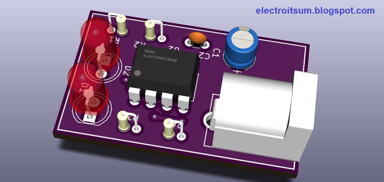
7. After the all above operations now, you can see
3D view of your PCB and for that go to view and then 3D viewer.
Gerber File:
1. Gerber is very important file because using this
file you can order your PCB to any PCB manufacturing company. For generating
these files we are going to use plot tool and for that go to file>plot. In plot
window select type as Gerber as shown in the below image. Now select all the layers for which you want to generate Gerber file like if your PCB uses 2 layers
F.Cu. and B.Cu. then select these layers. Also select the layer like front silk
and back silk if you have used. Now click on plot that will generate Gerber
file for layers, but not for drill.


2. For generating drill file click on the "generate
drill file" and after that select the drill file format as Gerber then click on "drill file" and "map file" which will generate their respective files. These files can be found in their
respective project directory.

OUTPUT 3D:

In the next tutorials, we will learn how to create own custom schematic symbol.
----------------------------------------------------------------------------------------------------------------------------------------------
You may also like:-
Arduino with GLCD
IoT with ESP8266

OUTPUT 3D:

In the next tutorials, we will learn how to create own custom schematic symbol.
----------------------------------------------------------------------------------------------------------------------------------------------
You may also like:-
Arduino with GLCD
IoT with ESP8266