Pages

Tuesday, April 28, 2020

KiCad (PCB Layout)

In this tutorial, we will continue the previous tutorial where we were discussed about how to design a schematic of the circuit.
1. Open kicad and then go to tools> run pcbnew. You will find a new black coloured window which is nothing but a PCB editor or layout editor tool. Now we have to read the netlist which we were created in the previous tutorial, for importing the components in this PCB layout designer. So go to tools and then click on netlist a small window will open in which you have to click on read button after that close the window. In the PCB editor window, you will find the whole components that we were used in the previous tutorial or footprint that we have assigned to our components in the previous tutorial.


2. Now we have to arrange all the components according to our board size or need. You will find that all components are connected to each other by threads. These threads are generated by kicad to show the connections which we created in schematic designing part. Here we can use some keyboard shortcut like if you want to move any text or footprint then simply hover the mouse on it and press "M" now you can move component easily. If you want to edit its properties then simply press ‘E’ and for rotate press ’R’.


3. Now after arranging all components start tracing with the help of track and via tool which you will find the right side of the window and also you can select working layer like front copper or back copper from the toolbar as shown in the below image. Remember you can’t place track between two terminals which are not connected by a thread to each other. While tracing the tracks if you want to change the working layer then simply press ‘v’ it instantly switches the tracing layer and if you press again then it returns to previous working layer. This is very helpful when you are going to place a jumper or if you are unable to find out the clearance for your track.


4. If you want to change the default track width then you have to go design rules>design rules and you will find here various settings like track width, via dia, clearance, etc. you can change them according to your PCB needs. Using design rules you can also set up the working layers like your PCB is going to use 2 layers or more.


5. After tracing is done now we have to define the outer edge of the PCB. This step is very important because it will provide the dimension of the PCB as well as it is also necessary for generating the 3D view of PCB. For that select Edge Cuts from the right sidebar (Layers) where you selected the PCB working layer and select pointer as "graphical line and polygons" as shown in the below image. Now simply draw the rectangle which encloses your components, remember don’t draw the line over track and also don’t leave too much space otherwise your PCB will look bulky and not optimized.


6. After enclosing a few things are remaining before we can jump to the Gerber file generating step. If you want to fill the unused space by copper you have to use the tool ‘add filled zones’. For adding simply select the pointer from the right side as shown in the image then draw a rectangle which encloses your entire PCB (including edge cuts mark). When you start drawing rectangle a small window will open which asks you to select the layer and a pad which is going to be sorted with fill zone, commonly ground pad is preferred. After that hover your mouse on the rectangle and click right button then select fill zone, you will get the layout as shown in the below image.


Similarly, you can also add a fill zone to another side layer.


7. After the all above operations now, you can see 3D view of your PCB and for that go to view and then 3D viewer.

Gerber File:
1. Gerber is very important file because using this file you can order your PCB to any PCB manufacturing company. For generating these files we are going to use plot tool and for that go to file>plot. In plot window select type as Gerber as shown in the below image. Now select all the layers for which you want to generate Gerber file like if your PCB uses 2 layers F.Cu. and B.Cu. then select these layers. Also select the layer like front silk and back silk if you have used. Now click on plot that will generate Gerber file for layers, but not for drill.


2. For generating drill file click on the "generate drill file" and after that select the drill file format as Gerber then click on "drill file" and "map file" which will generate their respective files. These files can be found in their respective project directory.
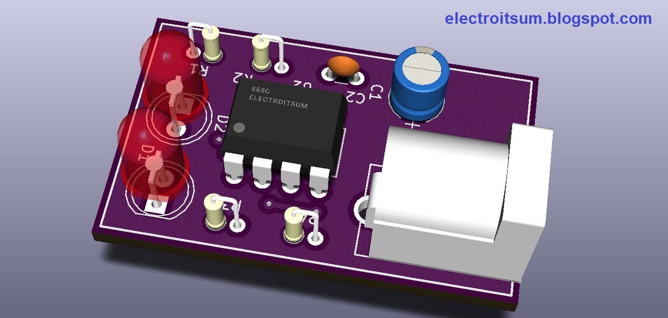


OUTPUT 3D:


 In the next tutorials, we will learn how to create own custom schematic symbol.
----------------------------------------------------------------------------------------------------------------------------------------------
You may also like:-

Arduino with GLCD

IoT with ESP8266

Saturday, April 25, 2020

Smoke detection using AT89C51


Hello guys, hope you are here because you want to make something or gain some electronics knowledge so let’s start DIY-
In this DIY session, we will discuss about the smoke detector using one of the simplest microcontrollers, 8051 which is made by Atmel Company. In this DIY project you need the following things –
  • 16X2 LCD Display
  • 10K pot
  • 10k Resistor
  • 8.2k resistor
  • Push-button
  • Buzzer
  • 11.0592 MHz Crystal Oscillator
  • 22pf capacitor – 2
  • 5v power supply
1. AT89CXX:

This is one of the simplest microcontrollers which can be used for small projects. 8051 series microcontrollers came into existence early 90s and first was made by the Intel Company. It has various functions like, it has built-in UART for serial communication, two types of interrupt hardware and software, RAM, ROM, an oscillator circuit, 16-bit timer, etc. This microcontroller has four 8bit general-purpose I/O port.


2. MQ5:

MQ5 is a smoke detector sensor which can be used for smoke, carbon monoxide as well as flammable gas detection. There are various types of sensors available in this “MQ” series and they have different sensing and functionality. You can buy an MQ5 module for this project because it gives calibration facility as well as 2 types of output digital and analog output. Digital output is simply used for the detection purpose whereas analog output used for detection as well as monitoring the level of smoke. Here we are going to use simple digital output because we are not going to measure the level of smoke density. For better understanding find the below image. In the below image, you can see the blue colour variable resistor which is used for the calibration process and you can simply adjust this according to your need like you want to detect very rare or denser smoke. And don’t increase sensitivity too much because it can give our circuit a false trigger.


3. 16X2 LCD:

16X2 is an alphanumeric LCD display which is widely used in embedded systems because it is very easy to interface with any microcontrollers. 16X2 LCD has 2 rows and 16 columns so that you can display 32 characters on display at a time. This display provides various other functionalities like you can on or off the cursor, you can choose cursor type, you can address DDRAM, custom character, read or write, backlight brightness control, etc. In this project, we will use a 10k pot for display backlight control. We will discuss the complete procedure of LCD interfacing in a different tutorial.


4. Power supply:

For 8051 we have to use 5v power supply and if you don’t have then simply connect the 9v battery using voltage regulator ic7805. The circuitry for 7805 is given below. If you are going to use power supply then check its output before connecting to the circuit because high voltage can damage our controller and here we are not going to use any type of high voltage protection.


5. Working:

The working of project and circuit is very simple when the MQ5 sensor detects any smoke or flammable gas it instantly gives a low output at the DO pin. This output is detected by the I/O pin of the microcontroller and then it is processed for further work and manipulation. Remember for mounting the sensor with microcontroller use pull-up resistor for preventing false detection. Here we will show the status of the smoke sensor on the LCD so microcontroller read the status and write its status on LCD. If the status is normal then LCD shows smoke absent and when detected then write smoke detected and turn on the buzzer. Here in the circuit design we used a button (Highlighted in red circle) in the place of the sensor so replace it with the MQ5 sensor. Circuit is shown below.


6. Code:

Here we are using assembly language to code the microcontroller and code is so simple. We continuously monitor the pin P3.7 which is connected to the smoke sensor and gives the low-level output after detecting the smoke. When microcontroller detects the low level on the pin it starts writing a status on the LCD and set 0 the buzzer pin so that buzzer starts beeping. For detecting a single pin status we are going do logical OR operation with port data to 01111111 binary data which gives the two possible outcomes 11111111 or 01111111 and we compare this data to predefined data for the port when we detect smoke or in a simple word we masked the whole bit expect P3.7.  After detecting smoke you have to reset the microcontroller for stopping buzzer and restart the program. The code is given below.


#############################################################################################################################
$mod51
org 00h
MOV P2,#38H
ACALL CMD 
MOV P2,#06H
ACALL CMD
MOV P2,#01H
ACALL CMD
MOV P2,#00FH
ACALL CMD 
ACALL delay
mov P2,#'S'
Acall dat
mov P2,#'M'
Acall dat
mov P2,#'O'
Acall dat
mov P2,#'K'
Acall dat
mov P2,#'E'
Acall dat
mov P2,#' '
Acall dat
mov P2,#'A'
Acall dat
mov P2,#'B'
Acall dat
mov P2,#'S'
Acall dat
mov P2,#'E'
Acall dat
mov P2,#'N'
Acall dat
mov P2,#'T'
Acall dat
loop:
CLR A
MOV A, P3
ORL A, #01111111B
CJNE A, #11111111B, DET
SJMP loop
DET:
MOV P2,#01H
ACALL CMD
mov P2,#'S'
Acall dat
mov P2,#'M'
Acall dat
mov P2,#'O'
Acall dat
mov P2,#'K'
Acall dat
mov P2,#'E'
Acall dat
mov P2,#' '
Acall dat
mov P2,#'D'
Acall dat
mov P2,#'E'
Acall dat
mov P2,#'T'
Acall dat
mov P2,#'E'
Acall dat
mov P2,#'C'
Acall dat
mov P2,#'T'
Acall dat
mov P2,#'E'
Acall dat
mov P2,#'D'
Acall dat
mov P2,#'!'
Acall dat
CLR P3.6
EMR: SJMP EMR
CMD:
CLR P3.0
CLR P3.1
SETB P3.2
ACALL DELAY
CLR P3.2
RET
dat:
SETB P3.0
CLR P3.1
SETB P3.2
ACALL DELAY
CLR P3.2
RET
delay:mov r0,#10
h0:mov r1,#20
h1:mov r2,#20
h2:djnz r2,h2
djnz r1,h1
djnz r0,h0
ret
end

#############################################################################################################################

7. OUTPUT:


#############################################################################################################################

You May Like:-

      - ARDUINO with GLCD
     
          -Know Your Arduino


Friday, April 24, 2020

KiCad (Schematic Designing)


          Kicad is a free software for electronic design automation (EDA). It is an advanced software for designing PCBs and you can design multilayer PCBs free of cost even up to 32 layers and it uses an integrated environment for designing PCB Layouts or schematics. Kicad was developed by Jean-Pierre. This software provides various tools like Bill of Materials, Gerber file ad, 3d prototype viewer, etc. kicad also provides the facility of adding custom components by designing your own schematics and footprint. So without wasting our time let’s start our first tutorial in which we are going to learn how to design your schematics in kicad.


1. Open your kicad software which will look like as below given screenshot. After that go to file and create a new project. you can give project name as you want. At the end of the process, kicad asks you “Do you want to create a new empty directory of the project?” and choose yes, because it is a good practice to put all project files in a specific directory and it also prevents the missing file problems.

2. Now in the PCB designing process, first of all, we have to create a schematics of the project or in a simple language, we have to represent our whole circuit in symbolic form. For that we have to access the schematic editor and we can do it in three ways.
a.      By sidebar
b.      By upper bar
c.      By Tool menu


3. Now double click on filename.sch from sidebar and after that, a new window will open which is known as electronic schematic editor (Eeschema), and here we will draw our schematic circuit. For placing the component choose place component tool from the sidebar as shown in the screenshot.


4. Start placing components after selecting the tool. It will ask you to choose the component which is going to be placed. Select your component as shown in the below screenshot.


5. After placing all components you have to connect them according to the circuit design and for that choose wire tool from the sidebar and then click on the first pin which you want to connect after that click on the next pin where we want to terminate wire connection. Similarly do all connections.


6. After all connections, our schematic design is done now we have to go through some steps for converting this schematic circuit into PCB layout. And for that first of all we have to annotate the schematic and for that go-to tool menu and click on annotate schematic and simply click on annotate (we will discuss options in different tutorials). Annotating is a procedure where we assign a unique name to our used components serial wise like first IC “U1” and second IC as “U2” and so on. Kicad can do all this work by itself using the annotating schematic tool.


7. After annotation, we are ready to assign footprints to our schematic symbols used in our design. In footprint assigning procedure we simply assign the device package type we are going to use in PCB. This step is very important because here you tell to kicad that we are going to use which type of components. For example, let consider you used 555 ic in your schematic but when you are going to create layout then how software treat 555 ic, is it SMD or THT package? And this type of problem is resolved by assigning footprint to schematic symbols.


8. For assigning footprint go-to tools and then assign component footprint. Now here a window will open with a list of used components, click on the component and after that open the footprint library which is situated on the left side of the component list. You will find the all possible footprint at the right side of the component list choose the footprint by double-clicking on it and the system will assign that footprint to the component which you selected. If you want to view how footprint actually looks like then simply select footprint and then click on "view selected footprint" tool as shown in the screenshot. Similarly assign footprint to all components.


9.  After assigning footprint we have to generate netlist and this will be our last step in creating the schematic design. netlist generation is an important step because it generates all the connections that we have done in the schematic circuit for layout design. For generating netlist we will use a netlist generating tool and for that go to tools and then go to generate netlist file after that simply click on generate it will ask you for the place where you want to save netlist file and save it in respective directory. After this save the schematic and we are ready to go for layout design which we will discuss in the next tutorial.


----------------------------------------------------------------------------------------------------------------------------------------------------------

Tuesday, March 31, 2020

IoT with ESP8266


IoT is an advanced technology for monitoring or controlling the electronics systems by using the internet as a medium. Nowadays we are searching for a medium that can be easily available for all users as well as has a wide range of coverage. The Internet is one of the media which is available for almost every person and it has a wide range of coverage even over the seas. Here we are going to discuss the simplest IOT project where we will use nodemcu which is a microcontroller board with a built-in esp8266 Wi-Fi interface and control an LED using a button and get its status on the LCD screen. For controlling our microcontroller based system we will use an android application named “Blynk”.
So let’s start setting up our Blynk app.
Blynk:
Nodemcu is a microcontroller board with built-in Wi-Fi. Nodemcu board can be programmed using Arduino ide and for that, we have to just download libraries for nodemcu and add preferences but we are not going to discuss how to setup nodemcu, here we are going to discuss how to setup Blynk. For adding libraries for Blynk follow the following step –
1.       Open Arduino ide
2.       Sketch
3.       Include library
4.       Manage libraries
5.       Search for Blynk
6.       Install the first result


Now Install the Blynk app from the play store on your mobile and open it. At first, you have to login, in this, you have to give an email id in which the authentication key will be sent. This key is very essential for linking your app to your project.

After login, you have to create a new project by pressing + sign (New Project) button. Then you have to give a name to your project and select the board like it is raspberry pi, esp8266, or any other IoT boards. Here we are going to use esp8266 so select it. After that click on the create button. Now we will get a message regarding to authentication key which is sent to the registered email-id. After that this we will get an empty project and now we can add various widgets in this empty project like buttons, sliders, LCD display LED, etc.


For adding those we have to tap on + sign at the upper right corner and you will get all the things that we need in the current project and here we are going to add an LCD screen and a button for controlling the led. After choosing the widgets (LCD or button) tap on it and here you can configure it for LCD screen toggle the LCD control type simple to advance after that LCD requires only one pin (virtual) for controlling it and in this project select virtual pin 1 (V1).  Now move on the button, tap on the button, and set digital pin gp5 as output pin actually, all digital and analog pins chosen in the app give output at respective gpio pin on board.


Here all the settings of our app are completed now we can move on to our board programming section.  The programming section is very simple, first of all, we have to put authentication key which was sent on registered email-id, after that give to internet access by giving SSID (Wi-Fi name) and password. Here we are using serial communication for getting information about the connection status of the board whether it is connected to the internet or not and it is optional. Now in the setup section first of all clear the LCD screen and put the initial values (status of led). In the loop section we continuously monitor the button status and send the status on LCD. Here we are using if-else because we want to print the led status only one time for one status (on or off) otherwise it won’t print properly because of the loop and very high refresh rate. Flash the program on your nodemcu board and in the app tap the play button located at the top right corner and wait for the successful internet connection, you can monitor the connection using serial monitor of the Arduino IDE if your board is connected to the computer by USB cable. After successful connection your first IoT project ready for test!!

here is the code for this project:-


--------------------------------------------------------------------------------------------------------------------------

#define BLYNK_PRINT Serial
#include <ESP8266WiFi.h>
#include <BlynkSimpleEsp8266.h>

WidgetLCD lcd(V1);
int status1 = 0;
int x = 0;                     //flag for current led status

char auth[] = "Auth Key";         // your authentication key from mail


char ssid[] = "SSID";         // your wifi name
char pass[] = "PASSWORD";    //your wifi password

void setup()
{
  // for checking connection
  Serial.begin(9600);

  Blynk.begin(auth, ssid, pass);
  lcd.clear();
    lcd.print(0, 0, "Electroitsum");
  lcd.print(0, 1, "LED:     OFF");
}

void loop()
{
  Blynk.run();
  status1 = digitalRead(D1);   // read pin status
  if(status1 == HIGH){                      //for led on
    if(x == 0){
    lcd.clear();
    lcd.print(0, 0, "Electroitsum");
     // (position X: 0-15, position Y: 0-1, "Message you want to print")
  lcd.print(0, 1, "LED:     ON");
  delay(10);
  x = 1;
    }
 }

  else{
    if(x == 1){                                  //for led of
    lcd.clear();
  // (position X: 0-15, position Y: 0-1, "Message you want to print")
  lcd.print(0, 0, "Electroitsum");
  lcd.print(0, 1, "LED:     OFF");
  delay(10);
  x = 0;
    }
  }
}
--------------------------------------------------------------------------------------------------------------------------
Output:-

Sunday, January 26, 2020

Know Your Arduino

What is an Arduino?

Arduino is a simple open-source platform for prototyping your design. Nowadays Arduino is widely used by the tinkerer and hobbyist. Arduino Provides the best user Interface environment for users. Arduino gained its popularity because it is user-friendly and doesn’t require any type of external hardware for programming or installing. Most of the old development boards require external hardware which is known as a programmer but in the case of Arduino, you can simply plug a USB and program it. The first Arduino is manufactured in Italy.


Things that make an Arduino   

Arduino consist of various electronics elements for various purposes.  Actually, Arduino is just a Family name and this family has many members which can be differentiated by its size, work, hardware, etc. Here we will talk about Arduino Uno R3 because it is a standard board and widely used. We will also talk about other family members but in a different tutorial.


1. USB-B:


Arduino needs power for processing or doing its work and this can be done by using a USB B type cable in Arduino UNO. By using this cable we can provide power supply from any USB socket available in the computer or communication link board. Actually, the power supply function is a secondary function of this socket. The primary function of this socket is to provide a medium by which we can feed program from our system (Laptop or Computer) to Arduino. So we will use this USB B type socket for programming.


2. Power Supply (7v - 12v):


This is another socket which is used for supplying power. Usually, we provide power by using USB cable but think about a project where you have to put your Arduino outdoor and you don’t have any access of USB communication link then you have to provide power by using 12v adapter, which uses regular home supply and provides you 12v dc power supply. You can simply plug this adapter to Arduino for power-up.


3.Voltage Regulator IC:

There is a 3 pin IC which looks like a transistor With heat sink but actually, it is a voltage regulator IC which is used for maintaining the ambient voltage range for proper working. The exact work of this IC can be seen when we apply 9 – 12v supply by power socket but as we know the board works on 5v so we have to provide 5v by any mean and the most suitable mean, is to regulate the voltage to 5v by using a 5v voltage regulator ic.


4. Xtal Oscillator:


Crystal Oscillator here used for as always for generating clock signal which is used by the microcontroller for time reference. Here board uses a 16 MHz Crystal Oscillator.


5. ATMega 16:


This is a QFN Package IC manufactured by ATMEL and known as ATMega 16 which is an 8-bit microcontroller. Basically, this microcontroller is not for users, it is used for handling the USB interface.


6.RESET BUTTON:


This is a hardware button that is used for resetting the board. This button forces the microcontroller to stop executing the current programs and start executing the program from the Initial program address. In other words, execute the program from start.


7.Built-In Led Pin:


In Arduino Board, you will find a Built-in Led which is connected to pin no 13. This Led or Pin 13 can be used for monitoring or indicating any specific task.


8. Tx and Rx LED:


There is a pair of LED you will find next to the built-in led. This Pair of LED known as the Tx and Rx led pin which indicates the status of transmitting or receiving data.


9.Serial Tx and Rx pin:


Pin 0 and 1 Known as Rx Tx pin respectively. These 2 pins are used to transmit or receive data serially from external devices. Pin 0 is used for receiving whereas pin 1 is used for transmitting the data. The above two LEDs actually indicate the status of these two pins. These pins also can be used as simple digital I/O pins.  

10. On Indication LED:


In the Arduino board, we will find a green LED beside the ICSP pins. This LED is used to indicate the power status of the board. If the board has sufficient power supply then it glows otherwise it stays in the off state.

11.  ATMega 328:


This is an 8-bit microcontroller that is manufactured by Atmel and known as ATMega 328.This a 28 pin microcontroller that works on 5v supply. Basically, this controller is available for the user, whatever the program we feed to controller goes to this microcontroller. This microcontroller has various built-in functions like one serial port, two hardware interrupt, 6 channels ADC (Analog to Digital Converter), 3 I/O ports, etc.      

12. ICSP Header Pin:


The bunch of pins situated at the end of the board known as ICSP pins. These pins are used for initial programming purposes or for uploading the firmware to the ATMega 328 microcontroller IC. Actually, microcontrollers read the binary and next layer assembly language but for conveying the specific Arduino ide command we have to load some initial commands which decode the Ide data according to the microcontroller and this commands or program is known as Boot program or boot command. 

13.Analog Pins

There are 6 (A0, A1, A2, A3, A4, A5) analog input pins which are connected to built-in ADC (Analog to Digital Converter). Sometimes we have to interface analog-type sensors which give analog output but our Arduino can process only on digital data so we have to convert that analog signal into their respective digital signal and that time we need this ADC. These pins also can be used as simple digital I/O pins. 

14. Digital I/O Pins

These 12 pins (2, 3, 4, 5, 6, 7, 8, 9, 10, 11, 12, 13) are our main concern because we are going to use these pins in almost our every project. These are simple Digital input and output pins which are work on defined job (input or output). In Arduino Uno, there are 6 pure digital pins (2, 4, 7, 8, 12, 13) in other words these pins have only digital input/output operation and don’t have any other specific tasks whereas remaining 6 pins (3, 5, 6, 9, 10, 11) have digital I/O as well as PWM (Pulse Width Modulation) operation. These 6 pins can be used as a PWM generator with an appropriate duty cycle and frequency.

15. Power Supply for Add-ons


There are various types of add-ons available in the market which works with the Arduino boards and generally these boards are known as "shield". These shields are maybe for sensors, motors or any other optoelectronics devices and they need power for their proper operation and this power can be supplied by using power output. Arduino Uno can provide 5v as well as 3.3v supply for external boards.  

Friday, January 3, 2020

ARDUINO with GLCD


Here we are going to interface a 128 x 64 graphical LCD which consists of two KS0108 LCD controllers. This GLCD widely used in embedded system products. First of all, if we want to interface a graphical LCD then we have to, learn some basic principles of LCD working. You can consider an LCD as an array of led lights if you want to show something on the display you have to on or off the led in the required pattern. The 128 x 64 led has 128 pixels or you can say led in a row whereas 64 pixels (led) in the column. Now we only need to access these LEDs to on-off them in a required manner.

The 128 x 64 led has 2 KS0108 controllers so let’s try to understand the working of these controllers in GLCD.  See the below image which represents the GLCD pixel map -


In the above image, you can easily find out that the first controller controls the first half of display from the left side and the second one, the second half of the display. The first controller is responsible for the 64 bits in y-direction as well as in x direction also here we can see that the first half display is divided into 8 segments which are known as “Page”. So the x direction 64 bit is divided into 8 segments of 8 bit or page.

If we want to display an image than we have to, put the pixel values of that image in according to this LCD pixel distribution. Now let’s see the pin configuration of the GLCD and which pin is useful for us.
As in the above image, there are 8 pins which are known as data pins (DB0 – DB7). These pins are used to transmit or receive 8-bit data between CPU (Arduino) and GLCD Controllers. There are 5 Control signal pins which we will use to convey the GLCD about our requirements. The CS1 and CS2 pins are active high pins which we will use for selecting the controller from the two controllers (KS0108). The DI pin is known as data/instruction pin, this pin is used for the convening GLCD that, the transmitted data on data pins is a data or an instruction. The R/W pin is read/write pin which acknowledges that the CPU is going to write data on LCD or going to read data from the LCD. When this pin is high it means that CPU is going to read data from LCD whereas if this pin is low then CPU is going to write data on LCD, That’s why we will connect it to the ground because here we want to write data on LCD only. The E Pin stands for Enable pin which acts as gate opener, so we have to give a small pulse every time whenever we want to transmit the data.


After setting up all hardware we have to prepare code for GLCD. Here we are going to write code without using any GLCD library of ARDUINO. If you have interfaced a 16 x 2 LCD then it is very easy for you to interface a GLCD, but if you don’t then don’t worry I am here. If you want to interface an LCD then you have to follow just only two steps, first is, initialize the LCD by giving initial commands and then start feeding the data which you want to show. Here I am giving the table below which is used for initializing the GLCD.


Here I have cross marked all unnecessary commands. First of all, we have to initialize the LCD but before that, we have to define some control signal pins and data pins which is given below-

//-------------------------------------------------------------------------------------------------//
#define data PORTD //port for 8 Bit data #define en 13 // defined control signal pins #define rs 12 #define cs1 10 #define cs2 11 int x = 0; // some variables that will be used in the programming int p = 0; int z = 0; byte img[] = {}; //Put HEX code of an 128x64 image
//------------------------------------------------------------------------------------------------//

The setup function will be like this -

//-----------------------------------------------------------------------------------------------//
void setup() { DDRD = DDRD|B11111111; // Setting up port D as a 8 bit data out port pinMode(en, OUTPUT); // setting up all control signal pins pinMode(rs, OUTPUT); pinMode(cs1, OUTPUT); pinMode(cs2, OUTPUT); lcdon(); // function call to initialize LCD setx(0xb8); // this function sets the initial address for x (row) sety(0x40); // this function sets the initial address for y (column) }
//-----------------------------------------------------------------------------------------------//

Here the three function named lcdon(), setx(), sety() will be discussed later. Let’s start coding the function which we will use. First of all, we are taking enable function which is nothing but a single high pulse generator. In this function, we will make enable pin high for a few mill seconds and then we will make it low. The code for this given below.

//-----------------------------------------------------------------------------------------------//
void enable(){ digitalWrite(en, HIGH); // make en pin high delay(0.5); //delay 0.5ms digitalWrite(en, LOW); // make enable pin low delay(0.5); //delay 0.5ms }
//-----------------------------------------------------------------------------------------------//

Next, we are going to take lcdon function. In this function, we will send the LCD on command to GLCD. For this, first of all, we will pull up the CS1 and CS2 pin high as we want to initialize both the part of GLCD. After that, we will make DI pin low because the data we want to send is a command not manipulating data which is going to display on the LCD. Here we are going to send 0x3f hex data which will initialize the LCD. The 0x3f hex is taken from initializing command data which is given above you can refer that. After all this, we are going to call enable function because it works like gate opener for the GLCD controller.

//-----------------------------------------------------------------------------------------------//
void lcdon(){ digitalWrite(cs1, HIGH); //select 1st KS0108 digitalWrite(cs2, HIGH); //select 2nd KS0108 digitalWrite(di, LOW); // make di low for command data = 0x3f; //glcd initializing hex data enable(); }
//-----------------------------------------------------------------------------------------------//

Similarly, we will send set the control signals in setx and sety function but just we will change the command hex code according to the function like for setting up x display address we will send 0xb8 which sets the x address to page 0 (First page).

//-----------------------------------------------------------------------------------------------//
void sety(byte datay){ digitalWrite(cs1, HIGH); //select 1st KS0108 digitalWrite(cs2, HIGH); //select 2nd KS0108 digitalWrite(di, LOW); //make di low for command data = datay; //set data which is hold by datax enable(); } void setx(byte datax){ digitalWrite(cs1, HIGH); //select 1st KS0108 digitalWrite(cs2, HIGH); //select 2nd KS0108 digitalWrite(di, LOW); // make di low for command data = datax; //set data which is hold by datax enable(); }
//-----------------------------------------------------------------------------------------------//

The value of datax and datay will be given by passing the value at the time of function call according to our needs.

The next functions are writ1 and writ2 which are used for holding the data into a variable from the image data array. The writ1 function holds the data from 0 to 63 for the first page of the first controller and writ2 holds the data from 64 to 127 of the next controller. Here we will pull up the DI signal pin as now the transmitted hex code is not a command.

//-----------------------------------------------------------------------------------------------//
void writ1(int c1){ digitalWrite(cs1, HIGH); //select first controller digitalWrite(cs2, LOW); // deselect the second controller digitalWrite(di, HIGH); // Pull up di high as the hex data is now not a command data = img[c1]; //copy img array data into "data" variable enable(); } void writ2(int c2){ digitalWrite(cs1, LOW); //deselect first controller digitalWrite(cs2, HIGH); // select the second controller digitalWrite(di, HIGH); data = img[c2]; enable(); }
//-----------------------------------------------------------------------------------------------//

Draw function is a very simple function which is used for placing the data into the display which was putted into a variable in the writ1 and writ2 functions. It uses 8 similar blocks for 8 rows or pages. It puts the value of image data one by one into their respective pixel address.


//-----------------------------------------------------------------------------------------------//
void draw(int p){ if(p==0){ //for first page for (x=0; x<64; x++){ // loop for 64 times writ1(x); //writ1 function call int y = 64+x; // for first page 2nd controller writ2(y); // call function writ2 } x=0; //reset the counter value } if(p==1){ // for page second setx(0xb9); // set the x address of second page sety(0x40); // set the y address of second page for (x; x<64; x++){ // loop for 64 times writ1(128+x); //writ1 function call int y = 192+x; // for second page 2nd controller writ2(y); // call function writ2 } x=0; } if(p==2){ // for page 3 setx(0xba); sety(0x40); for (x; x<64; x++){ writ1(256+x); int y = 320+x; writ2(y); } x=0; } if(p==3){ //for page 4 setx(0xbb); sety(0x40); for (x; x<64; x++){ writ1(384+x); int y = 448+x; writ2(y); } x=0; } if(p==4){ //for page 5 setx(0xbc); sety(0x40); for (x; x<64; x++){ writ1(512+x); int y = 576+x; writ2(y); } x=0; } if(p==5){ //for page 6 setx(0xbd); sety(0x40); for (x; x<64; x++){ writ1(640+x); int y = 704+x; writ2(y); } x=0; } if(p==6){ //for page 7 setx(0xbe); sety(0x40); for (x; x<64; x++){ writ1(768+x); int y = 832+x; writ2(y); } x=0; } if(p==7){ // for page 8 setx(0xbf); sety(0x40); for (x; x<64; x++){ writ1(896+x); int y = 960+x; writ2(y); } x=0; } }
//-----------------------------------------------------------------------------------------------//


//-----------------------------------------------------------------------------------------------//
byte img[] = { 0x00,0x00,0x00,0xFC,0x04,0x04,0x04,0x04,0x04,0x04,0x04,0x04,0x04,0x04,0x04,0xC4, 0x04,0x04,0x04,0x04,0x04,0x04,0x04,0x04,0x04,0x04,0x04,0x04,0x04,0x04,0x04,0x04, 0x04,0x04,0x04,0x04,0x04,0x04,0x04,0x04,0x04,0x04,0x04,0x04,0x04,0x04,0x04,0x04, 0x04,0x04,0x04,0x04,0x04,0x04,0x04,0x04,0x04,0x04,0x04,0x04,0x04,0x04,0x04,0x04, 0x04,0x04,0x04,0x04,0x04,0x04,0x04,0x04,0x04,0x04,0x04,0x04,0x04,0x04,0x04,0x04, 0x04,0x04,0x04,0x04,0x04,0x04,0x04,0x04,0x04,0x04,0x04,0x04,0x04,0x04,0x04,0x04, 0x04,0x04,0x04,0x04,0x04,0x04,0x04,0x04,0x04,0x04,0x04,0x04,0x04,0x04,0x04,0x04, 0x04,0x04,0x04,0x04,0x04,0x04,0x04,0x04,0x04,0x04,0x04,0x04,0x04,0xFC,0x00,0x00, 0x00,0x00,0x00,0xFF,0x00,0x00,0x00,0x10,0x30,0x30,0x50,0x90,0x10,0x18,0x07,0x00, 0x07,0x18,0x10,0x90,0x50,0x30,0x30,0x10,0x00,0x00,0x00,0x00,0x00,0x00,0x00,0x00, 0x00,0x00,0x00,0x00,0x00,0x00,0x00,0x00,0x00,0x00,0x00,0x00,0x00,0x00,0x00,0x00, 0x00,0x00,0x00,0x00,0x00,0x00,0x00,0x00,0x00,0x00,0x00,0x00,0x00,0x00,0x00,0x00, 0x00,0x00,0x00,0x00,0x00,0x00,0x00,0x00,0x00,0x00,0x00,0x00,0x00,0x00,0x00,0x00, 0x00,0x00,0x00,0x00,0x00,0x00,0x00,0x00,0x00,0x00,0x00,0x00,0x00,0x00,0x00,0x00, 0x00,0x00,0x00,0x00,0x00,0x00,0x00,0x00,0x00,0x00,0x00,0x00,0x00,0x00,0x00,0x00, 0x00,0x00,0x00,0x00,0x00,0x00,0x00,0x00,0x00,0x00,0x00,0x00,0x00,0xFF,0x00,0x00, 0x00,0x00,0x00,0xFF,0x00,0x00,0x00,0x00,0x00,0x00,0x30,0x1E,0x11,0x08,0x04,0x04, 0x04,0x08,0x11,0x1E,0x30,0x00,0x00,0x00,0x00,0x00,0x00,0x00,0x00,0x00,0x00,0x00, 0x00,0x00,0x00,0x00,0x00,0x00,0x00,0x00,0x00,0x00,0x00,0x00,0x00,0x00,0x00,0x00, 0x00,0x00,0x00,0x00,0x00,0x00,0x00,0x00,0x00,0x00,0x00,0x00,0x00,0x00,0x00,0x00, 0x00,0x00,0x00,0x00,0x00,0x00,0x00,0x00,0x00,0x00,0x00,0x00,0x00,0x00,0x00,0x00, 0x00,0x00,0x00,0x00,0x00,0x00,0x00,0x00,0x00,0x00,0x00,0x00,0x00,0x00,0x00,0x00, 0x00,0x00,0x00,0x00,0x00,0x00,0x00,0x00,0x00,0x00,0x00,0x00,0x00,0x00,0x00,0x00, 0x00,0x00,0x00,0x00,0x00,0x00,0x00,0x00,0x00,0x00,0x00,0x00,0x00,0xFF,0x00,0x00, 0x00,0x00,0x00,0xFF,0x00,0x00,0x00,0x00,0x00,0x00,0x00,0x00,0x00,0x00,0x00,0x00, 0x00,0x00,0x00,0x00,0x00,0x00,0x00,0x00,0x00,0xFE,0xFE,0x22,0x22,0x22,0x22,0x00, 0x00,0xFE,0xFE,0x00,0x00,0xE0,0xB0,0x90,0x90,0xB0,0xE0,0x00,0x00,0xE0,0x30,0x10, 0x10,0x30,0x00,0x10,0xF8,0xFC,0x10,0x00,0xF0,0xF0,0x10,0x10,0x00,0xE0,0x30,0x10, 0x10,0x30,0xE0,0x00,0x00,0xF6,0xF6,0x00,0x10,0xF8,0xFC,0x10,0x00,0xF0,0xD0,0x90, 0xB0,0x00,0x00,0xF0,0xF0,0x00,0x00,0xF0,0xF0,0x00,0x00,0xF0,0xF0,0x10,0x10,0xF0, 0xE0,0x10,0x10,0xF0,0xE0,0x00,0x00,0x00,0x00,0x00,0x00,0x00,0x00,0x00,0x00,0x00, 0x00,0x00,0x00,0x00,0x00,0x00,0x00,0x00,0x00,0x00,0x00,0x00,0x00,0xFF,0x00,0x00, 0x00,0x00,0x00,0xFF,0x00,0x00,0x00,0x00,0x00,0x00,0x00,0x00,0x00,0x00,0x00,0x00, 0x00,0x00,0x00,0x00,0x00,0x00,0x00,0x00,0x00,0x07,0x07,0x04,0x04,0x04,0x04,0x00, 0x00,0x07,0x07,0x00,0x00,0x03,0x06,0x04,0x04,0x06,0x02,0x00,0x00,0x03,0x06,0x04, 0x04,0x06,0x00,0x00,0x07,0x07,0x04,0x00,0x07,0x07,0x00,0x00,0x00,0x03,0x06,0x04, 0x04,0x06,0x03,0x00,0x00,0x07,0x07,0x00,0x00,0x07,0x07,0x04,0x02,0x06,0x04,0x04, 0x07,0x01,0x00,0x03,0x07,0x04,0x04,0x07,0x07,0x00,0x00,0x07,0x07,0x00,0x00,0x07, 0x07,0x00,0x00,0x07,0x07,0x00,0x00,0x00,0x00,0x00,0x00,0x00,0x00,0x00,0x00,0x00, 0x00,0x00,0x00,0x00,0x00,0x00,0x00,0x00,0x00,0x00,0x00,0x00,0x00,0xFF,0x00,0x00, 0x00,0x00,0x00,0xFF,0x00,0x00,0x00,0x00,0x00,0x00,0x00,0x00,0x00,0x00,0x00,0x00, 0x00,0x00,0x00,0x00,0x00,0x00,0x00,0x00,0x00,0x00,0x00,0x00,0x00,0x00,0x00,0x00, 0x00,0x00,0x00,0x00,0x00,0x00,0x00,0x00,0x00,0x00,0x00,0x00,0x00,0x00,0x00,0x00, 0x00,0x00,0x00,0x00,0x00,0x00,0x00,0x00,0x00,0x00,0x00,0x00,0x00,0x00,0x00,0x00, 0x00,0x00,0x00,0x00,0x00,0x00,0x00,0x00,0x00,0x00,0x00,0x00,0x00,0x00,0x00,0x00, 0x00,0x00,0x00,0x00,0x00,0x00,0x00,0x00,0x00,0x00,0x00,0x00,0x00,0x00,0x00,0x00, 0x00,0x00,0x00,0x00,0x00,0x80,0x80,0x80,0x80,0x80,0x80,0x80,0x80,0xC0,0x30,0x0E, 0x0C,0x30,0xC0,0x80,0x80,0x80,0x80,0x80,0x80,0x80,0x80,0x00,0x00,0xFF,0x00,0x00, 0x00,0x00,0x00,0xFF,0x00,0x00,0x00,0x00,0x00,0x00,0x00,0x00,0x00,0x00,0x00,0x00, 0x00,0x00,0x00,0x00,0x00,0x00,0x00,0x00,0x00,0x00,0x00,0x00,0x00,0x00,0x00,0x00, 0x00,0x00,0x00,0x00,0x00,0x00,0x00,0x00,0x00,0x00,0x00,0x00,0x00,0x00,0x00,0x00, 0x00,0x00,0x00,0x00,0x00,0x00,0x00,0x00,0x00,0x00,0x00,0x00,0x00,0x00,0x00,0x00, 0x00,0x00,0x00,0x00,0x00,0x00,0x00,0x00,0x00,0x00,0x00,0x00,0x00,0x00,0x00,0x00, 0x00,0x00,0x00,0x00,0x00,0x00,0x00,0x00,0x00,0x00,0x00,0x00,0x00,0x00,0x00,0x00, 0x00,0x00,0x00,0x00,0x00,0x00,0x01,0x01,0x02,0x04,0xE4,0x18,0x80,0x80,0x40,0x40, 0x40,0x40,0x80,0x80,0x18,0xE4,0x04,0x02,0x01,0x01,0x00,0x00,0x00,0xFF,0x00,0x00, 0x00,0x00,0x00,0x3F,0x20,0x20,0x20,0x20,0x20,0x20,0x20,0x20,0x20,0x20,0x20,0x20, 0x20,0x20,0x20,0x20,0x20,0x20,0x20,0x20,0x20,0x20,0x20,0x20,0x20,0x20,0x20,0x20, 0x20,0x20,0x20,0x20,0x20,0x20,0x20,0x20,0x20,0x20,0x20,0x20,0x20,0x20,0x20,0x20, 0x20,0x20,0x20,0x20,0x20,0x20,0x20,0x20,0x20,0x20,0x20,0x20,0x20,0x20,0x20,0x20, 0x20,0x20,0x20,0x20,0x20,0x20,0x20,0x20,0x20,0x20,0x20,0x20,0x20,0x20,0x20,0x20, 0x20,0x20,0x20,0x20,0x20,0x20,0x20,0x20,0x20,0x20,0x20,0x20,0x20,0x20,0x20,0x20, 0x20,0x20,0x20,0x20,0x20,0x20,0x20,0x20,0x20,0x23,0x21,0x21,0x20,0x20,0x20,0x20, 0x20,0x20,0x20,0x20,0x21,0x21,0x23,0x20,0x20,0x20,0x20,0x20,0x20,0x3F,0x00,0x00 }; // sample image array
//-----------------------------------------------------------------------------------------------//

___________________________________________________________________________________________________________________________

I have putted all my efforts to convey the GLCD interfacing with Arduino but, if you want more help for better understanding then feel free to comment and ask for the help and if you also think anything is wrong then you can tell me.

___________________________________________________________________________________________________________________________

For You!

KiCad (PCB Layout)

I n this tutorial, we will continue the previous tutorial where we were discussed about how to design a schematic of the circuit. 1...